- 您现在的位置:买卖IC网 > Sheet目录2008 > MAX1202AEPP+ (Maxim Integrated Products)IC ADC 12BIT 8CH 20-DIP
MAX1202/MAX1203
5V, 8-Channel, Serial, 12-Bit ADCs
with 3V Digital Interface
14
______________________________________________________________________________________
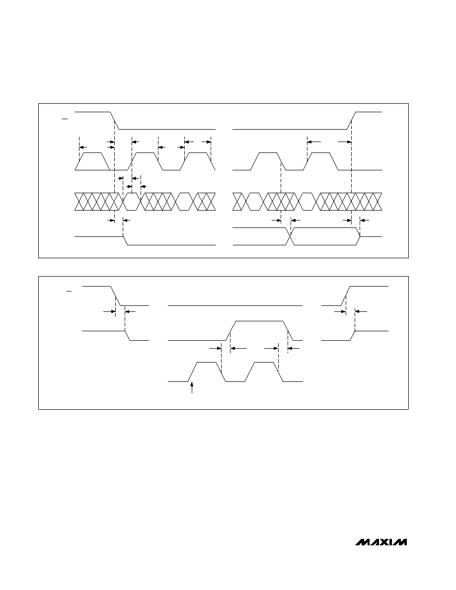
Figure 8. External Clock Mode SSTRB Detailed Timing
tSDV
tSSTRB
PD0 CLOCKED IN
tSTR
SSTRB
SCLK
CS
tSSTRB
Figure 7. Detailed Serial-Interface Timing
CS
SCLK
DIN
DOUT
tCSH
tCSS
tCL
tDS
tDH
tDV
tCH
tDO
tTR
tCSH
The conversion must complete in some minimum time or
droop on the sample-and-hold capacitors might degrade
conversion results. Use internal clock mode if the clock
period exceeds 10s or if serial-clock interruptions could
cause the conversion interval to exceed 120s.
Internal Clock
In internal clock mode, the MAX1202/MAX1203 generate
their own conversion clock. This frees the P from run-
ning the SAR conversion clock, and allows the con-
version results to be read back at the processor’s
convenience, at any clock rate from zero to 2MHz.
SSTRB goes low at the start of the conversion, then goes
high when the conversion is complete. SSTRB is low for
a maximum of 10s, during which time SCLK should
remain low for best noise performance. An internal regis-
ter stores data while the conversion is in progress. SCLK
clocks the data out at this register at any time after the
conversion is complete. After SSTRB goes high, the next
falling clock edge produces the MSB of the conversion
at DOUT, followed by the remaining bits in MSB-first for-
mat (Figure 9). CS does not need to be held low once a
发布紧急采购,3分钟左右您将得到回复。
相关PDF资料
MAX121EAP+
IC ADC 14BIT 308KSPS 20SSOP
MAX1238MEEE+T
IC ADC 12BIT SERIAL 16-QSOP
MAX1240AEPA+
IC ADC 12BIT SERIAL 8-DIP
MAX1245BCPP
IC ADC SRL 12BIT 2.375V 20-DIP
MAX1249AEPE+
IC ADC 10BIT SERIAL 16-DIP
MAX1279AETC+
IC ADC 12BIT 1.5MSPS 12-TQFN
MAX1285BESA+T
IC ADC 12BIT 300KSPS 8-SOIC
MAX1302BEUG+
IC ADC 16BIT SRL 115KSPS 24TSSOP
相关代理商/技术参数
MAX1202BC/D
功能描述:模数转换器 - ADC RoHS:否 制造商:Texas Instruments 通道数量:2 结构:Sigma-Delta 转换速率:125 SPs to 8 KSPs 分辨率:24 bit 输入类型:Differential 信噪比:107 dB 接口类型:SPI 工作电源电压:1.7 V to 3.6 V, 2.7 V to 5.25 V 最大工作温度:+ 85 C 安装风格:SMD/SMT 封装 / 箱体:VQFN-32
MAX1202BCAP
功能描述:模数转换器 - ADC Integrated Circuits (ICs) RoHS:否 制造商:Texas Instruments 通道数量:2 结构:Sigma-Delta 转换速率:125 SPs to 8 KSPs 分辨率:24 bit 输入类型:Differential 信噪比:107 dB 接口类型:SPI 工作电源电压:1.7 V to 3.6 V, 2.7 V to 5.25 V 最大工作温度:+ 85 C 安装风格:SMD/SMT 封装 / 箱体:VQFN-32
MAX1202BCAP+
功能描述:模数转换器 - ADC 12-Bit 8Ch 133ksps 5V Precision ADC RoHS:否 制造商:Texas Instruments 通道数量:2 结构:Sigma-Delta 转换速率:125 SPs to 8 KSPs 分辨率:24 bit 输入类型:Differential 信噪比:107 dB 接口类型:SPI 工作电源电压:1.7 V to 3.6 V, 2.7 V to 5.25 V 最大工作温度:+ 85 C 安装风格:SMD/SMT 封装 / 箱体:VQFN-32
MAX1202BCAP+T
功能描述:模数转换器 - ADC 12-Bit 8Ch 133ksps 5V Precision ADC RoHS:否 制造商:Texas Instruments 通道数量:2 结构:Sigma-Delta 转换速率:125 SPs to 8 KSPs 分辨率:24 bit 输入类型:Differential 信噪比:107 dB 接口类型:SPI 工作电源电压:1.7 V to 3.6 V, 2.7 V to 5.25 V 最大工作温度:+ 85 C 安装风格:SMD/SMT 封装 / 箱体:VQFN-32
MAX1202BCAP-T
功能描述:模数转换器 - ADC RoHS:否 制造商:Texas Instruments 通道数量:2 结构:Sigma-Delta 转换速率:125 SPs to 8 KSPs 分辨率:24 bit 输入类型:Differential 信噪比:107 dB 接口类型:SPI 工作电源电压:1.7 V to 3.6 V, 2.7 V to 5.25 V 最大工作温度:+ 85 C 安装风格:SMD/SMT 封装 / 箱体:VQFN-32
MAX1202BCPP
功能描述:模数转换器 - ADC RoHS:否 制造商:Texas Instruments 通道数量:2 结构:Sigma-Delta 转换速率:125 SPs to 8 KSPs 分辨率:24 bit 输入类型:Differential 信噪比:107 dB 接口类型:SPI 工作电源电压:1.7 V to 3.6 V, 2.7 V to 5.25 V 最大工作温度:+ 85 C 安装风格:SMD/SMT 封装 / 箱体:VQFN-32
MAX1202BCPP+
功能描述:模数转换器 - ADC 12-Bit 8Ch 133ksps 5V Precision ADC RoHS:否 制造商:Texas Instruments 通道数量:2 结构:Sigma-Delta 转换速率:125 SPs to 8 KSPs 分辨率:24 bit 输入类型:Differential 信噪比:107 dB 接口类型:SPI 工作电源电压:1.7 V to 3.6 V, 2.7 V to 5.25 V 最大工作温度:+ 85 C 安装风格:SMD/SMT 封装 / 箱体:VQFN-32
MAX1202BEAP
功能描述:模数转换器 - ADC RoHS:否 制造商:Texas Instruments 通道数量:2 结构:Sigma-Delta 转换速率:125 SPs to 8 KSPs 分辨率:24 bit 输入类型:Differential 信噪比:107 dB 接口类型:SPI 工作电源电压:1.7 V to 3.6 V, 2.7 V to 5.25 V 最大工作温度:+ 85 C 安装风格:SMD/SMT 封装 / 箱体:VQFN-32